


– ASML’s breakthrough in 1000-watt EUV light source technology could boost wafer throughput by 50% by 2030, cementing its lead in advanced chip fabrication.
– Lithography machines are the most complex and costly equipment in semiconductor production, accounting for up to 30% of chip manufacturing expenses.
– China’s domestic lithography efforts, spearheaded by Shanghai Micro Electronics Equipment (SMEE), face significant hurdles in EUV sources, high-NA optics, and dual-stage systems despite progress in DUV technology.
– The global lithography market is a triopoly dominated by ASML, with Nikon and Canon competing in lower tiers, creating strategic dependencies and investment risks in the semiconductor supply chain.
– For investors in Chinese tech equities, understanding lithography advancements is key to assessing opportunities in domestic semiconductor stocks amid geopolitical tensions and import restrictions.
The Pinnacle of Chip Making: Why Lithography Machines Matter
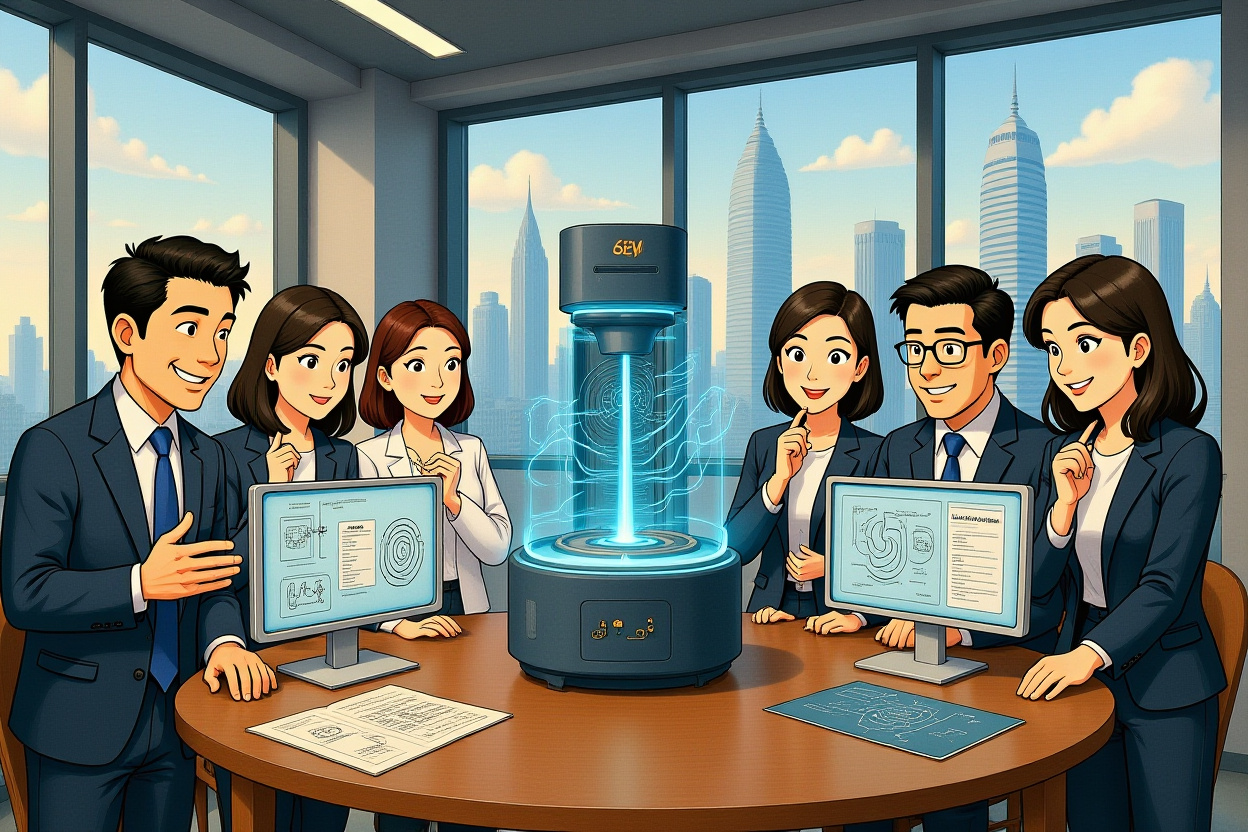
In the relentless pursuit of Moore’s Law, the lithography machine stands as the semiconductor industry’s most formidable challenge. This equipment, often described as the “Mount Everest” of manufacturing, directly dictates the pace of technological progress. A recent breakthrough by ASML—achieving a stable 1000-watt extreme ultraviolet (EUV) light source—highlights the relentless innovation driving this field. For global investors monitoring Chinese equity markets, the trajectory of lithography technology isn’t just an engineering marvel; it’s a critical determinant of supply chain security, corporate valuations, and national technological sovereignty.
The lithography machine’s role is unambiguous: it projects intricate circuit patterns onto silicon wafers, defining the transistors that power everything from smartphones to AI servers. As chip nodes shrink below 7 nanometers, the complexity and cost of these machines escalate exponentially. China’s ambitious push for semiconductor self-sufficiency, underscored by import restrictions on advanced lithography equipment, makes this a focal point for market analysts. The performance of domestic champions like Shanghai Micro Electronics Equipment (上海微电子装备公司) and their ability to scale the lithography summit will significantly influence the risk profile of Chinese semiconductor stocks.
Core Physics: The Rayleigh Criterion and Resolution Limits
At the heart of every lithography machine lies the Rayleigh criterion, a fundamental principle governing resolution. Expressed as CD = k1 • λ / NA, it defines the minimum feature size (CD) achievable based on light wavelength (λ), numerical aperture (NA), and a process factor (k1). To cram more transistors onto a chip, manufacturers must shorten wavelengths, increase NA, or reduce k1. ASML’s EUV machines use a 13.5nm wavelength, a drastic reduction from the 193nm of deep ultraviolet (DUV) systems, enabling 3nm process nodes. This physics-bound race explains why lithography machines are so costly and difficult to master, with each advancement pushing the limits of material science and precision engineering.
For China, mastering these principles is a non-negotiable step toward advanced chip production. While domestic design capabilities have reached 5nm, the manufacturing gap persists largely due to lithography constraints. The Rayleigh criterion isn’t merely academic; it’s the bedrock upon which investment decisions in fabless companies versus integrated device manufacturers must be evaluated. As Chinese firms like SMEE develop their own lithography machines, their success hinges on innovating within these physical boundaries, whether through new light sources or enhanced optics.
Global Lithography Landscape: ASML’s Hegemony and Competitive Dynamics
The global market for lithography machines is a stark oligopoly, with ASML holding over 60% share by value and a complete monopoly in EUV systems. Japanese giants Nikon and Canon account for most of the remainder, focusing on DUV and older technologies. In 2024, the trio shipped 683 units worth approximately $264 billion, with ASML delivering 201 of the 212 high-end EUV and ArFi systems. This concentration creates profound supply chain vulnerabilities, especially for Chinese chipmakers reliant on imported equipment. The lithography machine isn’t just a tool; it’s a strategic asset controlled by a handful of non-Chinese entities, influencing everything from Huawei’s smartphone revival to China’s AI chip aspirations.
ASML’s dominance stems from decades of strategic choices, such as embracing immersion lithography in the 2000s after TSMC’s former R&D vice president Lin Benjian (林本坚) proposed using water to enhance resolution. This move outflanked Nikon’s pursuit of a 157nm F2 light source, showcasing how collaboration with key customers can alter competitive fortunes. Today, ASML’s EUV machines integrate about 100,000 components from over 5,000 global suppliers, including Germany’s ZEISS for optics and the US’s Cymer for light sources. This distributed innovation model makes replicating ASML’s success exceptionally challenging, underscoring why China’s lithography ambitions require a holistic, ecosystem-driven approach rather than isolated breakthroughs.
EUV Lithography: The Crown Jewel and Its Guarded Secrets
Extreme ultraviolet lithography represents the apex of current technology, enabling chip geometries below 7nm. ASML’s EUV machines, costing over $300 million each, utilize a laser-produced plasma (LPP) source where high-power CO2 lasers strike tin droplets to generate 13.5nm light. The system’s complexity is staggering: mirrors must have atomic-level smoothness, with surface roughness below 0.02 nanometers, and the entire optical path operates in a vacuum to prevent EUV absorption. For Chinese firms, developing a comparable EUV lithography machine is a multi-decade endeavor, fraught with intellectual property barriers and export controls under agreements like the Wassenaar Arrangement.
Recent reports suggest that Chinese researchers are exploring alternative EUV source technologies, such as discharge-produced plasma (DPP) or the steady-state micro-bunching (SSMB) concept proposed by Tsinghua University. However, these remain in laboratory stages. The commercial reality is that ASML’s 1000W EUV source breakthrough, promising 330 wafers per hour by 2030, widens the gap further. Investors tracking Chinese semiconductor equities must weigh the likelihood of domestic EUV success against the timeline of ASML’s roadmap, which includes High-NA EUV systems with 0.55 numerical aperture for 2nm chips. The lithography machine’s evolution will directly impact the valuation of Chinese foundries like Semiconductor Manufacturing International Corporation (SMIC) and their ability to compete in advanced nodes.
China’s Domestic Lithography Endeavor: Progress Amidst Profound Challenges
China’s quest for lithography self-sufficiency is a cornerstone of its “02 Special Project” (国家科技重大专项), aimed at reducing reliance on foreign semiconductor equipment. The lead entity, Shanghai Micro Electronics Equipment (SMEE), has made tangible strides, notably with its 90nm dry DUV lithography machine, the SSA600/20, which entered the market in 2018. This machine, primarily used for back-end packaging and testing, demonstrates competence in mid-range technology. However, moving to the forefront requires conquering immersion DUV (ArFi) and eventually EUV systems. A 28nm lithography prototype has reportedly been delivered for testing, but industry observers caution that achieving high yield rates for production could take 3 to 5 years of tuning.
The gaps are multifaceted. In light sources, China produces DUV excimer lasers but lacks commercially viable EUV sources. For optics, domestic mirror surface roughness is around 0.5nm, compared to ASML’s 0.02nm, limiting resolution. Dual-stage systems, essential for high throughput, remain in laboratory phases. Moreover, supporting materials like high-end photoresists for ArF and EUV are overwhelmingly imported from Japan and the US. As People’s Bank of China Governor Pan Gongsheng (潘功胜) has emphasized financial support for tech innovation, these bottlenecks highlight that lithography machine development is as much about materials science and supply chain integration as it is about optics. For investors, this means monitoring a broad array of Chinese suppliers, from lens makers to chemical companies, rather than just equipment assemblers.
Key Components: Where China Stands in the Lithography Value Chain
Breaking down the lithography machine into its core subsystems reveals both strengths and vulnerabilities in China’s ecosystem. The light source, often called the “heart” of the machine, is a critical hurdle. While companies like Beijing Optoelectronics have made progress in DUV lasers, EUV requires a leap to LPP technology, involving precision tin-droplet targeting and power management that only ASML and Japan’s Gigaphoton have mastered. The optics, supplied globally by ZEISS, demand unparalleled polishing and coating techniques. Chinese institutes have achieved 30nm shape accuracy for mirrors, but mass production at EUV standards remains distant.
The dual-stage system, which allows simultaneous measurement and exposure to boost throughput, is another frontier. ASML’s TWINSCAN technology enables accelerations up to 7g and positioning accuracy below 2nm. Chinese academia, through collaborations like Tsinghua University’s research, has developed laboratory-stage stages with 10nm precision, but industrial application lags. Additionally, computational lithography software—essential for designing complex masks—relies on tools from US firms like Synopsys and Cadence, though domestic alternatives are emerging. Each component’s development timeline affects when a fully indigenous advanced lithography machine might emerge, informing investment horizons in related Chinese equities.
Technological Evolution: From g-line to High-NA EUV and Beyond
The history of lithography machines is a chronicle of relentless parameter optimization, guided by the Rayleigh criterion. Early systems used mercury lamps emitting g-line (436nm) and i-line (365nm) light, enabling chips down to 250nm. The shift to excimer lasers—KrF (248nm) and ArF (193nm)—ushered in the DUV era, supporting nodes to 65nm. The pivotal innovation was immersion lithography, where water between the lens and wafer effectively shortens the wavelength to 134nm, allowing single-patterning down to 28nm and, with multiple patterning, to 7nm. This lithography machine advancement underscores how incremental improvements can yield generational leaps, a lesson for Chinese engineers pursuing stepwise progress.
Today, the frontier is EUV, with High-NA EUV systems poised to enter production. ASML’s Twinscan NXE:5000 series, with a 0.55 NA, aims for 2nm chips. Beyond that, hyper-NA concepts exist but face prohibitive costs. For China, catching up may involve parallel paths: refining DUV multiple patterning for near-term needs while investing in next-generation technologies like nanoimprint lithography (NIL) or directed self-assembly (DSA). These alternatives, though less mature, could offer “leapfrog” opportunities if EUV proves too entrenched. Market participants should watch for R&D announcements from Chinese academies and state-backed consortia, as they could signal shifts in strategic focus that impact semiconductor sector valuations.
Light Source Advancements: The Wavelength Race
Shortening the light wavelength has been the primary driver of resolution gains. The progression from 436nm to 13.5nm involved moving from lamps to lasers to plasma sources. ASML’s recent 1000W EUV achievement, reported by Reuters, exemplifies this trajectory: by doubling tin-droplet frequency to 100,000 per second and optimizing laser pulses, power increases translate directly to higher wafer throughput. For Chinese developers, mastering DUV ArF excimer lasers is a prerequisite before tackling EUV’s complexities. Domestic firms like Changchun New Industries have capabilities in solid-state lasers, but the leap to high-power CO2 systems for EUV requires interdisciplinary expertise in physics, thermodynamics, and control systems.
Increasing Numerical Aperture and Computational Enhancements
Beyond wavelength, boosting numerical aperture (NA) through immersion fluids and larger lenses has been crucial. ASML’s immersion systems achieve NA of 1.35, near the practical limit. Concurrently, reducing the k1 factor via computational lithography—using AI to pre-distort mask patterns—has extended the life of older technologies. NVIDIA’s cuLitho software, developed with TSMC and ASML, accelerates these calculations 40-fold using GPUs. For China, investing in similar software capabilities is vital, as it can mitigate hardware limitations. The lithography machine of the future will increasingly rely on digital twins and machine learning, areas where Chinese tech firms like Huawei have competencies that could be leveraged.
ASML’s Blueprint: Collaboration, Acquisition, and Customer Alignment
ASML’s rise from a struggling joint venture in 1984 to a $300 billion behemoth offers a masterclass in strategic growth. Its success hinges on three pillars: deep supplier integration, customer co-investment, and open innovation. By acquiring critical suppliers like Cymer (EUV sources) and taking stakes in ZEISS (optics), ASML secured control over the lithography machine’s most delicate components. Its 2012 “Customer Co-Investment Program” brought in Intel, TSMC, and Samsung as shareholders, ensuring funding and guaranteed orders for EUV development. This model created a virtuous cycle where market leaders bankrolled the R&D that later benefited them exclusively.
For Chinese policymakers and corporate strategists, replicating this approach within the constraints of export controls is daunting but instructive. Building a domestic lithography ecosystem requires fostering similar collaborations among state-owned enterprises, private champions, and academic institutions. The “02 Special Project” attempts this, but scale and global connectivity are limited. Investors should evaluate Chinese semiconductor equipment firms not just on technical milestones but on their partnership networks—such as SMEE’s ties with the Chinese Academy of Sciences—as these relationships can accelerate progress. The lithography machine’s complexity means no single company can succeed alone; ecosystem health is a leading indicator of eventual success.
Lessons from the Nikon-ASML Rivalry
The historical contest between Nikon and ASML illustrates how strategic choices define market leadership. In the early 2000s, Nikon bet on 157nm F2 light sources, while ASML adopted immersion for existing 193nm ArF lasers. ASML’s lower-risk path, endorsed by key customers like TSMC, won out, consigning Nikon to a secondary role. For China, this underscores the importance of aligning technological roadmaps with market practicality. Pursuing exotic alternatives like electron-beam lithography may offer long-term potential, but near-term resources might be better spent mastering established DUV immersion, which still serves the majority of chip demand. This calculus affects investment allocations in Chinese tech funds, balancing speculative R&D with revenue-generating products.
Investment Implications for Chinese Semiconductor Equities
For institutional investors and fund managers focused on Chinese markets, the lithography machine narrative is a dual-edged sword. On one hand, China’s dependency on imported equipment poses a systemic risk, potentially capping the growth of advanced foundries and dampening valuations for stocks like SMIC or Hua Hong Semiconductor. On the other, nationalistic policies are funneling billions into domestic alternatives, creating opportunities in equipment makers, material suppliers, and design software firms. The lithography machine’s journey from blueprint to production line will ripple across sectors, influencing earnings forecasts and risk premiums.
Key areas to monitor include policy announcements from the Ministry of Industry and Information Technology (工业和信息化部), breakthroughs from SMEE or academia, and supply chain developments—such as local photoresist production. Additionally, geopolitical shifts, like US-led restrictions on DUV sales to China, could accelerate import substitution. Savvy investors might diversify across the semiconductor value chain, balancing exposure to lagging lithography efforts with strengths in packaging, testing, and mature-node manufacturing. The lithography machine isn’t merely a technical topic; it’s a barometer for China’s high-tech ambitions and a core variable in portfolio construction for Asia-focused equity funds.
Risks and Opportunities in a Fragmented Landscape
The risks are palpable: prolonged R&D cycles, intellectual property disputes, and potential technological obsolescence if global leaders like ASML advance rapidly. However, opportunities abound in niches where China already excels, such as back-end packaging lithography or legacy node equipment. Companies like NAURA Technology Group are making headway in etch and deposition tools, which could benefit from synergies with lithography development. Moreover, the push for lithography self-sufficiency is driving mergers and acquisitions within China’s tech sector, potentially creating national champions with integrated capabilities. Investors should maintain a long-term perspective, recognizing that lithography machine breakthroughs, if achieved, could trigger re-ratings across the semiconductor board, much as ASML’s EUV success propelled its market capitalization.
Navigating the Ascent: Strategic Patience and Market Realism
The lithography machine remains the semiconductor industry’s ultimate test of endurance and ingenuity. ASML’s dominance, built over decades through global collaboration, sets a high bar for any challenger. China’s determined climb, fueled by national strategy and vast resources, has yielded progress in mid-range technology but faces steep cliffs in EUV and advanced components. For market participants, this translates into a nuanced investment landscape: avoid overestimating near-term breakthroughs, but do not underestimate the long-term potential of a concerted, state-backed industrial push.
The path forward for Chinese semiconductor equities will be shaped by incremental wins—a new photoresist formulation, a better lens polishing technique, or a throughput improvement in existing machines. Investors should track these developments closely, engage with company management on R&D roadmaps, and consider diversified positions across the ecosystem. As the global chip race intensifies, the lithography machine’s evolution will continue to dictate who leads and who follows. Stay informed, stay strategic, and let data-driven analysis guide your allocations in this pivotal sector.